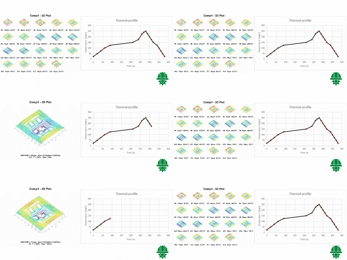
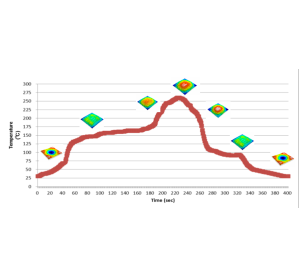
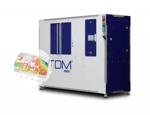
TDM (Topography Deformation Measurement) is a patented technology designed to the 3D measurements of complex objects under thermal stress. TDM exerts thermal profiles and cycles on electronics components in the same way as they are imposed on devices during production processes.
Understanding, simulating, and predicting the behavior of complex packages and boards during reflow is critical.

TDM helps the development and process engineer increase the reliability of his products, from simple components to highly complex packaging, and allows the failure analysis engineer to more accurately understand the root causes of failures observed in operations.
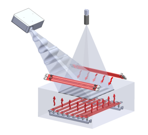
The TDM operating system combines a powerful, internally developed heating/cooling sequence with a sophisticated optical set-up for 3D topography analysis under thermal stress of all kinds of materials, components, and sub-systems. TDM can impose the same thermal profiles and cycles on the devices that they will actually experience during the production process and during regular use. TDM measures the 3D deformation related to the imposed thermal stress throughout the thermal cycle, thus revealing faults that would likely occur during normal production and use.
Thanks to its innovative patented technology and unique features, like sub-room chambers, scanning mode, multi-scale, and others, are the reason major companies have chosen the TDM system in electronics and semi-conductors for quality control and R&D purposes. TDM equipment is compatible with any existing topography tool on the market and can easily be integrated into all types of equipment.
Our customers acknowledged the technical advantages of the TDM system. Advantages like high-resolution sensors patented Multi-Scale, Scanning imaging plus the system’s versatility, and user-friendliness are functions that make the system stand out.


